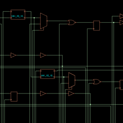
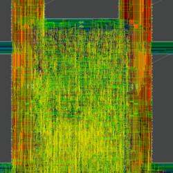
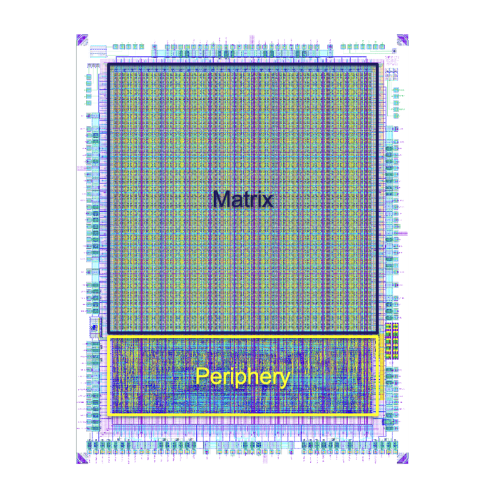
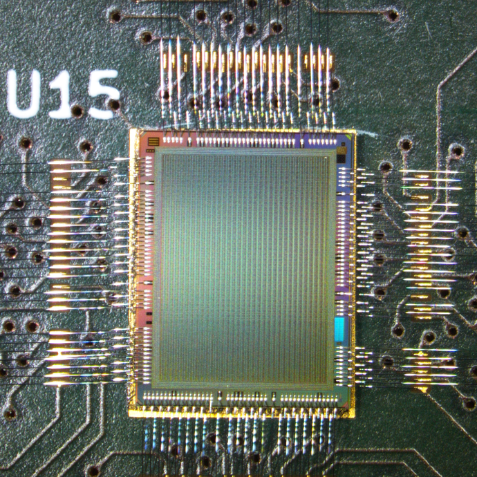
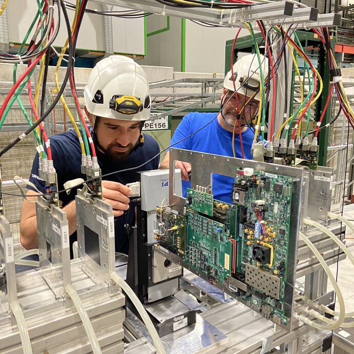
A research focus is on so-called Depleted Monolithic Active Pixel Sensors (DMAPS), in which the actual sensor and the previously separate CMOS-based front-end electronics are combined in one physical silicon die. Since high electrical voltages are usually required for charge collection, these types of detectors are also called HV-CMOS. This technology allows a very compact and ultra-light setup for vertex and tracking detector in HEP experiments. Thus it enables highly accurate measurements where unwanted multiple scattering in the detector is minimized.
The production of these detectors takes place in commercial chip factories (foundries), and is an expensive and lengthy process. For this reason, we are focussing in the design and simulation of these sensors, where the same tools are used as in the chip industry (Cadence, Cliosoft, Synopsis, Mentor,..). Since both analog electronics (charge collection in the detector part) and digital electronics (ADC, signal processing, storage) have to work together in a very small space, this task is very challenging. It requires detector knowledge, electronics knowledge and software expertise in equal measure.
Furthermore, we are also researching chip design based on open-source software (magic, KLayout,..) and using this with open-source PDKs like Skywater 130nm via the efabless initiative.
Research and Development within RD50

RD50 is a CERN R&D collaboration with main focus on the development of radiation-hard semiconductor devices for high luminosity accelerators. In recent years, this effort has also been extended to the development of monolithic active pixel sensors on high resistivity substrates. Currently, 17 institutes are working on ASIC design, TCAD simulations, DAQ system development, charaterization, and performance studies of the prototypes produced. HEPHY is one of these institutes and is taking the lead in ASIC digital design, FPGA firmware and DAQ system software development, as well as testing and studying the prototypes in the lab and in beam tests.
The latest prototype, the RD50-MPW3, is an HV CMOS chip in the LFoundry 150nm process with a pixel pitch of 62 μm, integrating both digital and analog readout electronics in each pixel. The 64 x 64 pixels on this chip are arranged in 32 dual columns and have optimized digital peripherals for efficient configuration and fast serial data transfer. Simulations show a power consumption of 22 μW per pixel and 9 ns time resolution.
Belle II VTX Upgrade: From Monopix to Obelix

Another current project is the development of an upgrade of the Belle II vertex detector based on DMAPS detectors.
An upgrade of the SuperKEKB accelerator is planned for the period 2026-2027, and a redesign of the interaction region is being considered. In addition, while the current Belle II vertex detector has shown excellent performance since data collection began in 2019, simulations show that the expected occupancy (number of active channels) at full accelerator luminosity exceeds the limits of current technology. For these reasons, the Belle II collaboration plans to completely replace the current DEPFET pixel and Si-strip-based vertex detector with a system based on CMOS pixel sensors.
The planned system will use DMAPS pixel sensors called OBELIX. It is based on existing prototypes called TJ-Monopix-2, which was developed in the past for other HEP applications. A vertex detector based on DMAPS technology will reduce the material budget and significantly improve the spatial resolution compared to the current detector. In addition, it will provide extreme improvement in occupancy compared to the current detector thanks to its fast readout architecture and small pixel dimensions of only 33x33 µm². In addition, a large on-chip hit buffer memory will support high trigger latency, allowing the implementation of more complex algorithms in the Belle-II trigger system.
DAQ systems development
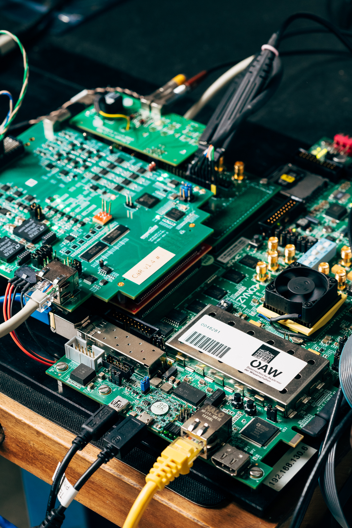
Data Acquisition (DAQ) systems refers to the set of electronics hardware, firmware, and software necessary to operate a detector and read out its data. These components, usually referred to as BE (back-end) electronics, must communicate with the actual (DMAPS) sensors and other FE (front-end) electronics. This includes the configuration of the FE electronics and DMAPS sensors, the slow control (measurement of voltages, currents, temperatures,..), as well as the transmission and processing of the actual pixel hit data from a high bandwidth data stream.
For the readout of the above mentioned RD50 and Belle-II Monopix/Opelix sensors we develop custom electronics, firmware for FPGAs and the high level software for this purpose. For the RD50 sensors, the so-called Caribou system is used, which is based on Xilinx Xynq 706 FPGA boards and communicates with the actual sensor-specific chip boards using special adapter boards (CaR boards). Our expertise here is again in digital design, development of low-level firmware that enables robust data transmission even at high bit error rates, and high-level firmware that enables live control of the data or integration with DAQ systems such as EUDAQ.
For the Belle-II OBELIX and TJ-Monopix2 sensors, a DAQ system based on the so-called BADAQ53 board is being used. This, as well as the above mentioned Caribou system, can be operated in our laboratories. Alpha or beta radiation from radioactive sources is used to induce signals in the DMAPS sensors. These measurements are usually used as preparation for beam tests at CERN, DESY, MedAustron or other accelerator centers.
