Understanding and controlling stresses in thin-films and during thermal annealing process is critical for achieving the desired optical, electronic and mechanical properties. Many of today´s high performance devices rely on or must be designed with “built-in” stresses within the individual layers to tailor specific characteristics. However, unwanted changes in stress can be introduced at any stage of the fabrication process, and may lead to a reduction in device performance as well as delamination or cracking of deposited films.
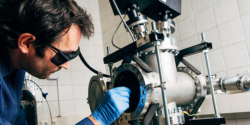
The Wafer Curvature techniques offers great possibilities of fast in-situ determination of film stresses during any thermal process in a non-destructive manner. Using a fast responding high-power resistive heating plate in a vacuum chamber, the measurement system is able to perform in-situ film stress measurements up to 1000°C at cooling and heating rates varying from 0.01 K/s up to several K/s.
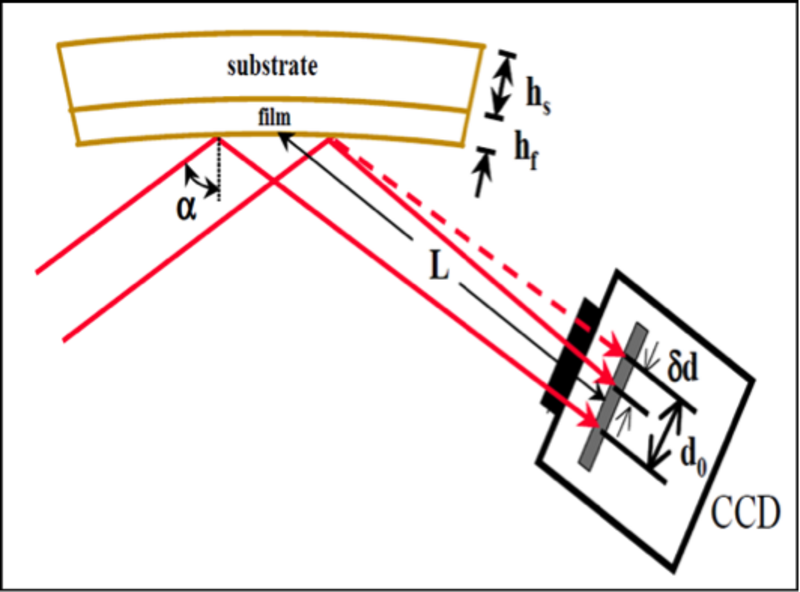
The two dimensional laser beam array enables in-situ film stress and curvature measurements for a wide range of metallic, ceramic and amorphous films. By using the known geometry and material properties of the substrate, the film the stress is calculated in real time by measuring the differential beam spacing δd/d0 caused by a bending of the film/substrate stack due to differences in film stress and thermal expansion coefficient. The high resolution of the differential beam spacing δd/d0ensures the high measurement sensitivity of about 6•10-5 GPa•µm stress-thickness product.