Setups for testing sensors, chips and test structures
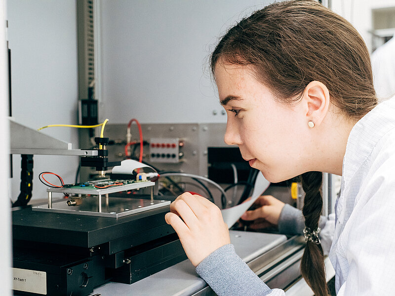
We operate various measuring apparatuses for the electrical characterization of silicon detectors in our clean rooms. These so-called "probe stations" are a proven tool for testing circuits and components on silicon wafers or bare silicon dies. Our setups were designed and built by the institute's workshop, thus optimally designed for testing silicon detectors.
For testing a sensor using such a probe station, it is placed on a so-called chuck and fixed by vacuum. The chuck is placed on a motorized table, which allows reaching different positions on the sensor. Metal needle tips allow to contact the sensor at any point and to establish electrical connections to various measuring instruments. Typical measurements are I-V, C-V curves, or resistivity or insulation tests. Automatic procedures by self-written software allow to scan through all strips/pixels of a sensor and perform these measurements repeatedly.
The following table lists the available probe stations:
| Setup Name | Anwendung | Tisch | Chuck | Meßgeräte |
| SQC | Automated strip scan on CMS Tracker sensors | motorized | room temp. | 2 SMU, Electrometer, LCR-Meter, Switching Matrix |
| PQC | Automated Test structure charaterization (CMS Tracker and HGCal) | motorized | temperature controlled | 2 SMU, Electrometer, LCR-Meter, Switching Matrix |
| HGCal | semi-automatic sensor tests, manual test structure tests | motorized | temperature controlled | 2 SMU, Electrometer, LCR-Meter, Switching Matrix |
| "P3" | manual measurements on diodes and simple test structures | motorized | room temp. | 2 SMU, Electrometer, LCR-Meter, simple IV/CV-Switch |
In addition, we have a climate chamber for aging studies and for operating sensors and detector modules at various temperatures (-40 to +200°C) and RF shielding boxes for studying noise and noise sources.
Setups for signal generation with lasers and radioactive sources
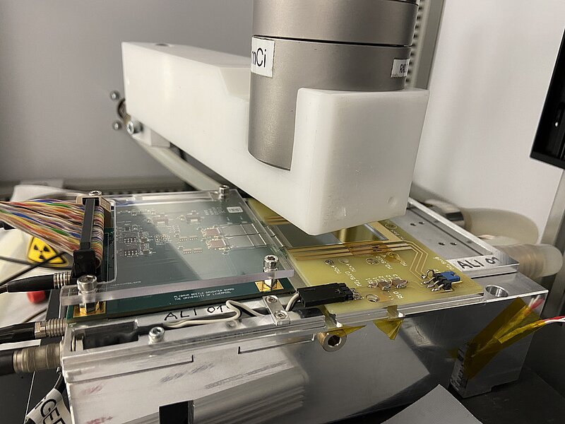
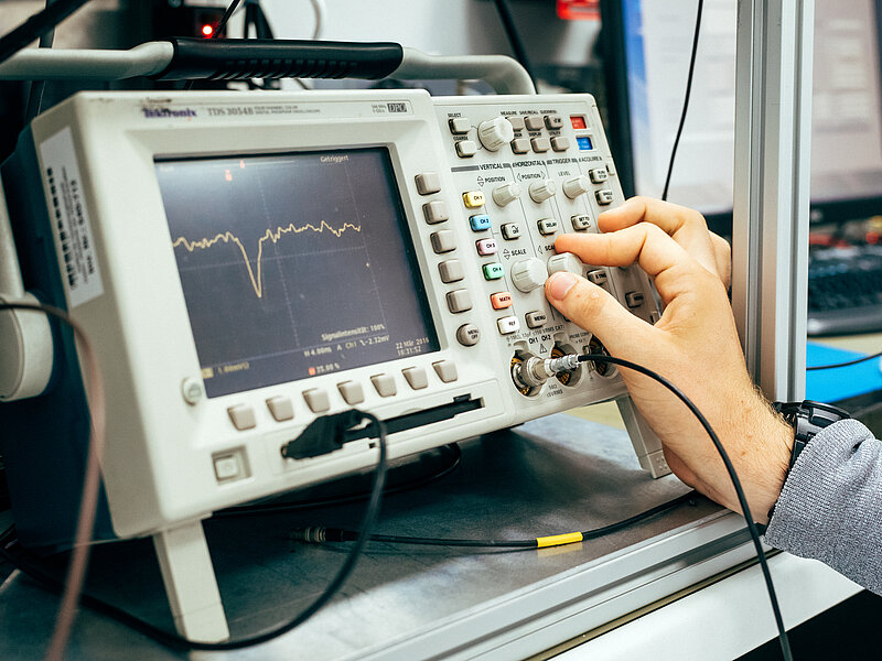
The Transient Current Technique (TCT) uses ultrashort laser pulses to mimic the passage of a particle. "Pilas" lasers from NKT with wavelengths of 1060nm, 833nm and 370nm are used. The last wavelength, which is in the UV range, is essential for investigating silicon carbide detectors. The electric current induced by each "pseudo" particle passage in the sensor is amplified (by devices from Cividec or the UCSC LGAD board, among others) and recorded with a fast oscilloscope. Rohde & Schwarz models with 16 GHz (RTP164) and 4 GHz (RTO6) bandwidth are available for this purpose. By examining the shape of the induced current, we can derive information about the detector's doping, electric field, and charge collection efficiency.
Complementing the laser pulses, radioactive sources are also used to record "real" particle transitions. Americium and strontium sources of various intensities are available for this purpose.
To study the charge partitioning in segmented detectors, we use the ALiBaVa system.
Detector construction and module assembly
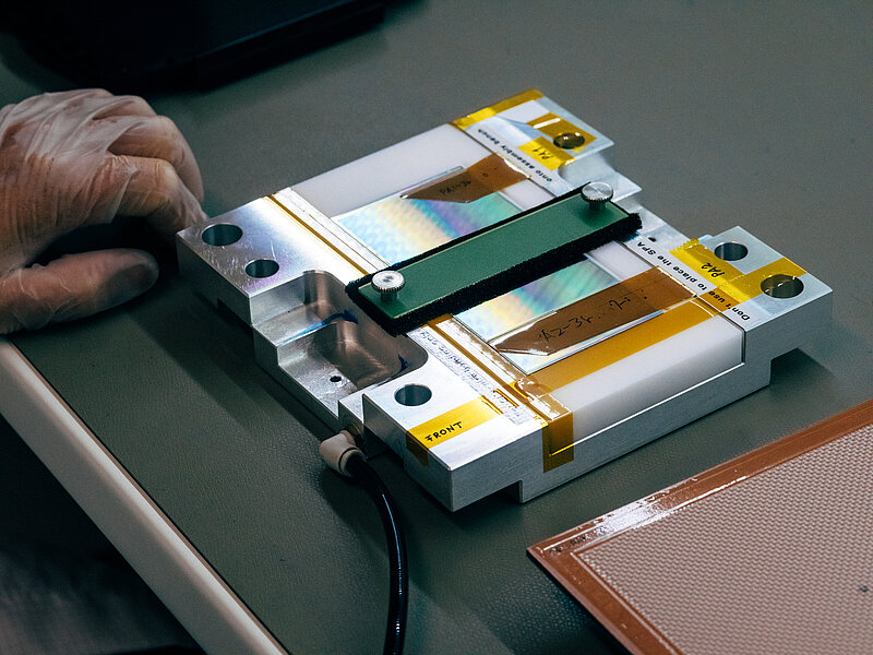
The construction of the CMS tracker required the assembly of about 17000 silicon strip detector modules, each consisting of silicon sensors and a readout hybrid bonded to a carbon fiber frame. About one thousand of these modules were fabricated at HEPHY. The so-called "Layer 4" of the Belle-II SVD was built here.
For both projects, it was necessary to build precision mechanics and special mounts ("jigs") in the institute's mechanical workshop. The actual assembly of the modules was done using a 3D coordinate measuring machine (Mitutoyo Euro-C776), to which we added the function of a gluing robot. This allowed the semi-automatic application of glue to the individual components of a module, as well as the quasi-simultaneous precise measurement of the position of the glued components.
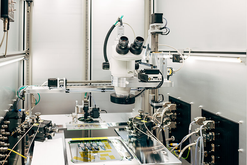
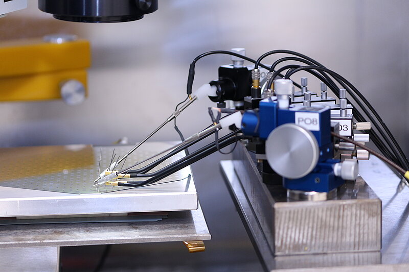
A fully automatic thin-wire bonder (Delvotec G5) is used to make the electrical connections between sensors, readout chips, and contact pads of the FE hybrids. A Dage pull tester is used for quality control of the wire bonds.
Several optical microscopes and a 3D microscope with confocal and interference technology (Leica DCM8) are available to visually inspect both the wire bonds and (sensor) surfaces.